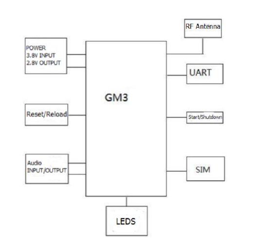
Hardware Design Introduction of GSM/GPRS Module USR-GM3
1.Typical Connection
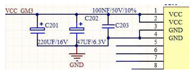
2.Power Interface
Working voltage VCC range from 3.4V-4.2V, 3.8V is recommended. Power the module by main power pin, pin interface is in parallel with appropriate energy-storage capacitance and high frequency capacitance.
Circuit diagram as follows
3.UART Interface
when the user MCU I/O level isn't 2.8V, it needs to make the level matching. DEVDD is the I/O power supply for customer MCU.V - PAD is the I/O power supply for GM3 module, users can use as UART matching and pull-up power.
Circuit diagram as follows:
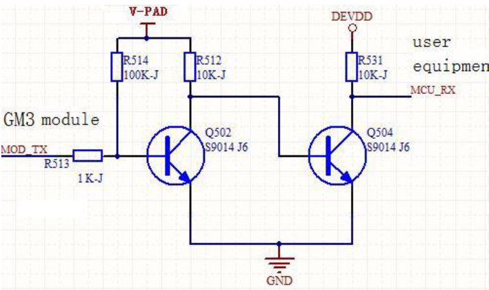
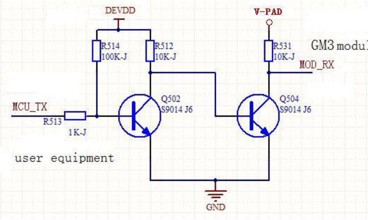
Note: when I/O power supply for customer MCU is 3.3v, MOD-RX pin of module don't have to level matching.
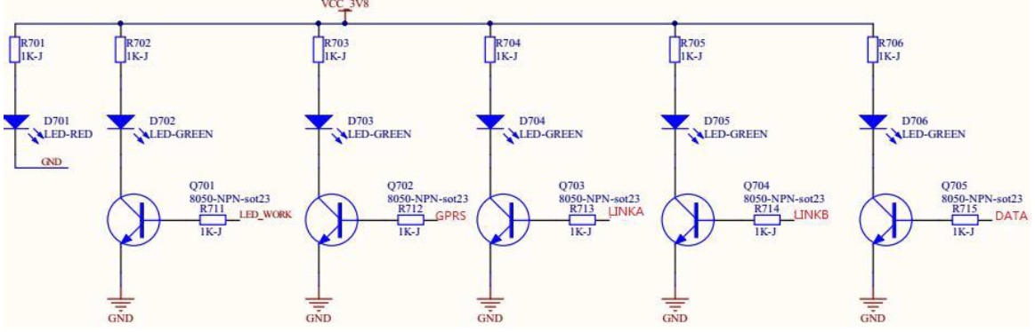
4.LED Output Control
The module provides LED output control and the module work status can be displayed by the LED status. Plusing power indicator is recommended.
Circuit diagram as follows:
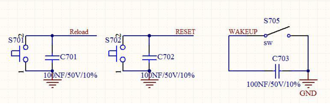
5.Reset, Reload and Wake up
Reload: Press 1s to 3s to restore user default settings, press over 6s to restore factory settings.
RESET: RESET pin connect to 10K pull-up resisitor. Press over 0.5s and release to reset the device.
WAKEUP:WAKE-UP pin connect to 10K pull-up resistor. Take effect in low level.
Circuit diagram as follows: